|
 об Обществе об Обществе
сотрудничество
есть идеи?
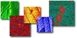
музей СЗМ
скан-галерея

|
МУЗЕЙ СЗМ
МУЗЕЙ СКАНИРУЮЩЕЙ ЗОНДОВОЙ МИКРОСКОПИИ И
НАНОТЕХНОЛОГИИ
Организаторы Музея заранее приносят свои извинения за
неполноту экспозиции и просят посетителей Музея присылать свои
замечания и экспонаты.
Отцы-основатели Сканирующей Зондовой
Микроскопии.
Создателями Сканирующей Зондовой Микроскопии
являются Binnig и Rohrer, удостоенные в 1986
году Нобелевской премии. Патент на Сканирующий Туннельный
Микроскоп был получен ими в 1982 году с приоритетом от
20.09.1979 г.
Heinrich Rohrer, left, and Gerd K. Binnig,
right, scientists at
IBM's Zurich Research Laboratory in Switzerland, are awarded
the 1986 Nobel Prize in physics for their work in scanning
tunneling microscopy. The researchers are recognized for
developing the powerful microscopy technique, which allows
scientists to view individual atoms on the surface of a
sample.
Фотография любезно предоставлена для нашего
музея Г. Биннигом.
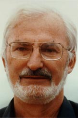 Heinrich Rohrer Heinrich Rohrer
Heinrich Rohrer, along with his colleague, Gerd K.
Binnig, was awarded the Nobel Prize in Physics in 1986 for his
work in scanning tunneling microscopy. Binnig and Rohrer were
recognized for developing the powerful microscopy technique,
which can form an image of individual atoms on a metal or
semiconductor surface by scanning the tip of a needle overthe
surface at a height of only a few atomic diameters.They shared
the award with German scientist Ernst Ruska, designer of the
first electron microscope.
Born in Buchs, Switzerland, on June 6,
1933, Dr. Rohrer was educated at the Swiss Federal Institute
of Technology in Zurich, where he received his bachelor's
degree in 1955 and his doctorate degree in 1960. After
post-doctoral work at the Swiss Federal Institute and Rutgers
University in the United States, Dr. Rohrer joined IBM's newly
formed Zurich Research Laboratory, studying, among other
things, Kondo materials and antiferromagnets before turning
his attention to scanning tunneling microscopy. Dr. Rohrer was
appointed an IBM Fellow in 1986, and was manager of the
physical sciences department at the Zurich Research Laboratory
from 1986 to 1988. He retired from IBM in July 1997. Last job
- Laboratory of Physics of small systems and Nanotechnology,
Calle Serrano 144 , Madrid 28006, Espana.
E-mail: h.rohrer@fsp.csic.es
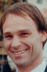
Gerd K. Binnig
Gerd K. Binnig, along with his colleague,
Heinrich Rohrer, was awarded the Nobel Prize in Physics in in
1986 for his work in scanning tunneling microscopy. Binnig and
Rohrer were recognized for developing the powerful microscopy
technique, which can form an image of individual atoms on a
metal or semiconductor surface by scanning the tip of a needle
overthe surface at a height of only a few atomic diameters.
They shared the award with German scientist Ernst Ruska,
designer of the first electron microscope.
Born in Frankfurt, Germany, on July 20,
1947, Dr. Binnig was educated at J.W. Goethe University in
Frankfurt, where he received his bachelor's degree in 1973 and
his doctorate degree in 1978. That year he joined a physics
research group at IBM's Zurich Research Laboratory. Dr. Binnig
was assigned to IBM's Almaden Research Center in San Jose,
Calif., from 1985 to 1986, and was a visiting professor at
nearby Stanford University from 1987 to 1988.
Dr. Binnig was appointed an IBM Fellow in1987 and remains a research staff member at IBM's ZurichResearch Laboratory.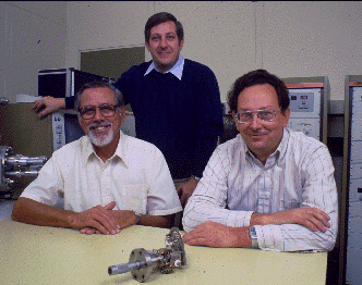
Необходимо, однако, отметить, что еще в1966 году Russel Young высказал идею о возможноститопографирования поверхности с помощью остроконечного зонда,который образовывал бы с ней туннельный контакт, а в 1971 годуопубликовал сообщение об инструменте, названном имTopografiner'ом, который содержал все основные узлы СТМ.
Russell Youngand his co-workers Fredric
Scireand John Ward (left to right) with theTopografiner.
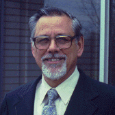
Russel Young
Russell D. Young obtained his B.S. degree in physics
from the Rensselaer Polytechnic Institute in 1953 and his
Ph.D. degree in physics from Pennsylvania State University in
1959. He remained at Penn State in the laboratory of Professor
Erwin Mueller for his postdoctoral research, which was marked
by several outstanding achievements. Among these were the
development of a high resolution field emission energy
analyzer and the first measurement of the total energy
distribution of field emitted electrons, as well as
contributions to the development of the low temperature field
ion microscope. He came to the National Bureau of Standards in
1961. His development of the Topografiner
was an outgrowth of his continued study of surfaces at NBS.
After the termination of this project in 1971, he remained at
NBS in both a technical and an administrative role until his
retirement in 1981. Since then he has actively pursued his
interests as an inventor, as a private consultant to industry
and government (including NIST), and as a grandfather and a
sailor.
Dr. Young's achievements have been
recognized in several awards. In 1974, he was the first
recipient of the Edward U. Condon Award, conferred by NBS in
recognition of outstanding scientific writing. He received the
U.S. Department of Commerce Silver Medal in 1979, a
Presidential Citation in 1986, and the Scientific Achievement
Award of the Washington Academy of Sciences in 1987. In 1992,
the American Vacuum Society recognized his invention of the
Topografiner by presenting him with the Gaede-Langmuir Award.
Описание Topografiner'а приведено в работах
( Phys. Rev. Lett. V. 27, N 14, 1971, P. 922-924. Full text.) ( Rev. Sc. Instr. V. 43, N 7,1972,
P. 999-1011. Full text.) , откуда взяты
приводимые ниже рисунки и комментарии к ним.
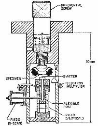 |
Present realization of the Topografiner. The
differential screw is used as a coarse adjustment to bring the
specimen close enough to the emitter so that it is within the
range of the vertical (Z) piezo. The X-scan piezo deflects the
emitter support post so as to scan the emitter in one
direction. The orthogonal (Y) piezo is not shown. The specimen
is clamped between copper blocks to permit heating. An
electron multiplier permits detection of secondary electrons. |
|
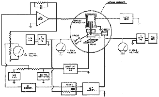
Block diagram for the Topografiner electrical
circuitry. The X-Y recorder is frequently replaced with a
memory oscilloscope which results in rapid scan rates with
somewhat reduced fidelily. The OPS bias permits positioning
the emitter at an appropriate distance from the surface.
Details of the servo loop are discussed in the
next. |
|
|
(a)
|
(b)
|
|
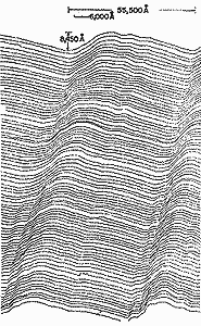
(a) Topographic map of a 180 line/mm diffraction
grating replica. This map was made with using an X-Y recorder.
Note the rippled surface at the base of the groove which may
have been caused by ruling instrument chatter or replica re-
moval. Details of the diamond tool used in the ruling engine
are evident. The emitter was kept about 200 A. above the
surface during these runs.
|
|
|
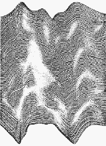
(b) Topographic map recorded on a memory oscilloscope
of a disturbed region of the same grating as (a). The vertical
magnification is about twice ihe horizontal magnifcation. The
contrast is reversed for easy comparison with (a). The close
spaced prohles give a highly desirable pictorial
representation of the surface topography. Mapping time—9
min.
|
|
|
Хотя
Young достиг на своем приборе разрешения в 3 А и указал на
возможность измерения одноатомных ступеней, ему все же не
хватило смелости предположить возможность получения
изображений отдельных атомов. Этой смелости хватило Binnig'у и
Rohrer'у - и они стали Нобелевскими лауреатами.
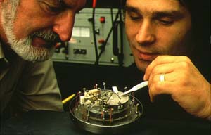
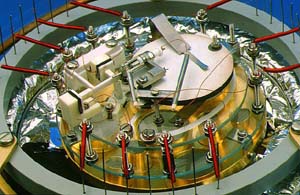
На фотографии точная копия первого сканирующего туннельного
микроскопа Биннига и Рорера (оригинал не сохранился).
Фотография любезно предоставлена для нашего музея Г.
Биннигом.
|
|
|
1982 год. Триумф сканирущей туннельной микроскопии -
изображение 7х7 реконструкции поверхности
кремния.
Зарождение и начальный этап развития туннельной
микроскопии прекрасно изложены в Нобелевской лекции Биннига и
Рорера. |
наверх
|